What Is an RF Switch and How Does It Work?

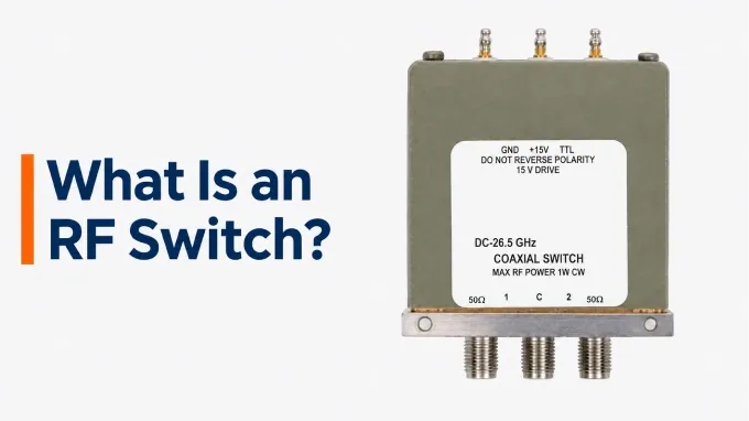
RF switches are devices that connect, disconnect, or select paths carrying RF signals. They change the signal route inside a circuit without requiring cables to be unplugged and reconnected. For example, a radio transceiver can use an RF switch to connect one antenna to either its transmitter or receiver.
How Does an RF Switch Work?
RF switches work by moving contacts or changing the electrical impedance of a switching element. This establishes the required connection while suppressing transmission through an unwanted path. The control input determines the switch’s state; it is separate from the RF signal being routed.
Unlike an RF power splitter, which distributes an input signal across multiple output paths, an RF switch selects which signal path is connected.
Electromechanical switches: An actuator, commonly an electromagnet, moves metal contacts together or apart. When the contacts meet, they form a conductive RF path. Separating them interrupts that path.
Solid-state switches: PIN diodes and FETs change impedance without moving contacts. Within its RF operating range, a PIN diode uses DC bias to control stored charge and RF resistance. Forward bias lowers that resistance; at zero or reverse bias, the diode behaves mainly as a small capacitance. In a FET, the voltage between gate and source controls conduction through the channel between source and drain.
RF MEMS switches: Microelectromechanical systems use microscopic moving structures to control RF transmission. Depending on the design, movement opens or closes a metal contact, or changes the capacitive coupling between two conductors. Both approaches change how the RF signal travels through the circuit.
Types of RF Switches
RF switches can be classified by their switching technology and by how they handle unused ports. These labels describe different characteristics: a PIN diode or FET switch can also be absorptive or reflective.
PIN Diode RF Switches
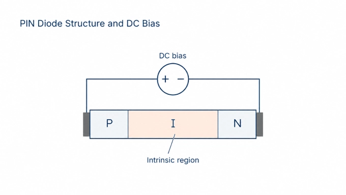
A PIN diode RF switch is a solid-state device whose switching elements are diodes with P-type, intrinsic, and N-type semiconductor regions. The applied DC bias controls the diodes’ RF impedance, allowing the switching circuit to establish or suppress RF transmission.
FET RF Switches
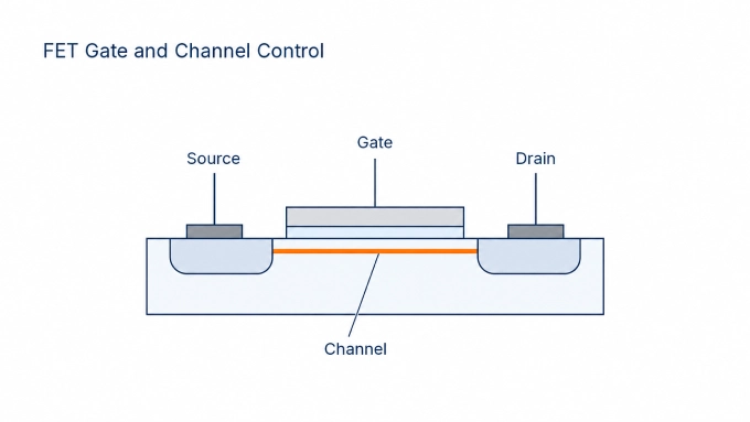
A FET RF switch is a solid-state device in which field-effect transistors control the connections between RF ports. Gate voltage determines the impedance of the transistor channels, enabling the circuit to pass or suppress RF signals without moving contacts.
Electromechanical RF Switches
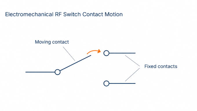
An electromechanical RF switch uses an electrically driven mechanism to move metal contacts, physically establishing or interrupting RF connections. The contacts and interconnections form a transmission path designed for a specified nominal impedance. An RF relay is a switch of this type.
RF MEMS Switches
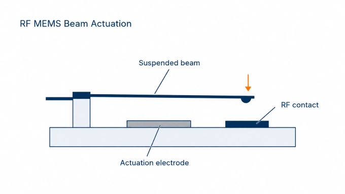
An RF MEMS switch uses a microscopic mechanical structure fabricated on a chip as its switching element. When actuated, the structure changes an electrical contact or capacitive coupling within the circuit. The switching action is mechanical, even though the device is manufactured using microfabrication techniques.
Absorptive vs. Reflective RF Switches
An absorptive RF switch, also called a terminated or nonreflective switch, connects designated inactive ports to loads that match the system impedance. In a 50 Ω system, these are nominally 50 Ω loads. They absorb incident RF energy and reduce reflections toward the connected source.
A reflective RF switch does not provide matched terminations for its inactive RF ports. Depending on the design and frequency, an unused port may resemble an open or short circuit. RF energy entering that port is largely reflected toward its source.
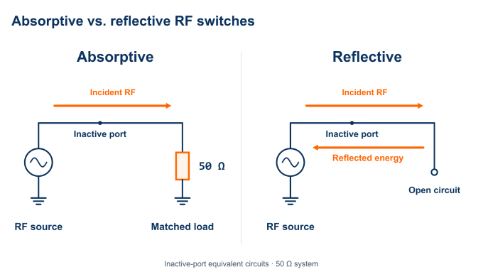
Absorptive switches suit systems that need a matched load at inactive ports; reflective switches suit systems that can tolerate reflected power. Absorptive designs must also dissipate energy in their termination loads, so an inactive port may have a lower power limit than the selected path.
Important RF Switch Specifications
RF switch specifications describe signal attenuation, leakage, matching, timing, power limits, and distortion.
Frequency range: The operating band sets the lower and upper frequencies over which the switch is specified. Both limits matter.
RF switch insertion loss: This measures attenuation through the selected path in dB. Lower loss preserves delivered power and helps protect receiver sensitivity when the switch precedes the low-noise amplifier. Attenuation can involve reflection as well as dissipation.
RF switch isolation: Isolation measures leakage attenuation between specified ports in a given state. Higher dB values mean less leakage. A high-isolation RF switch must meet the system’s leakage limit; there is no universal threshold for that label.
Impedance and matching: Nominal impedance is commonly 50 Ω or 75 Ω. Higher positive return loss and a voltage standing wave ratio (VSWR) nearer 1:1 indicate better matching and less reflection.
Switching and settling time: Switching time measures the response to a control change. Settling time describes how long the RF response takes to stabilize within a specified tolerance.
Power handling: Continuous-wave (CW) ratings apply to sustained RF power; peak ratings have specified pulse conditions. Hot-switching ratings apply during transitions with RF present; cold switching requires its removal. Also observe the internal termination limits described above.
Linearity: Compression increases attenuation at higher signal levels; intermodulation generates unwanted frequencies from multiple signals. P1dB marks 1 dB compression, while IIP3 characterizes third-order intermodulation. Neither is a maximum safe-power rating.
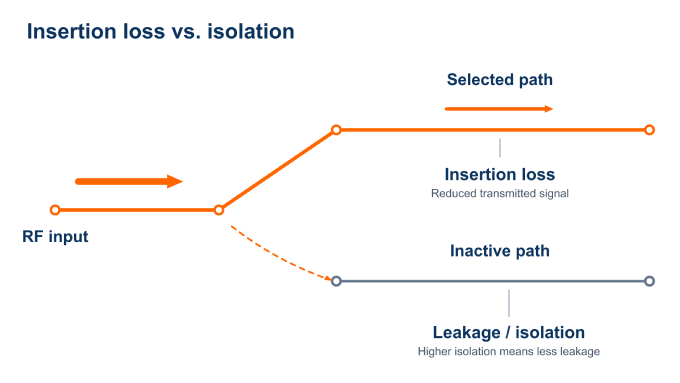
These parameters must be evaluated over the required operating frequency range rather than at a single test frequency. Check temperature, port pair, control state, and test conditions. Typical figures are not guaranteed limits, and connected equipment and interconnects can change installed performance.
What Makes a High-Isolation RF Switch?
A high-isolation RF switch is designed to suppress unwanted RF transmission while maintaining an acceptable signal path for the selected channel.
High isolation is commonly achieved through combinations of:
Series-shunt switching elements
Multiple cascaded switching stages
Low-parasitic device structures
Appropriate RF grounding
Careful circuit layout and electromagnetic isolation
Optimized impedance matching
There is no universal isolation threshold that defines a switch as high-isolation.
A 40 dB isolation specification may be sufficient in one system but inadequate in another, particularly when a high-power transmitter shares an RF network with a sensitive receiver.
How to Use RF Switches
Using an RF switch involves connecting the RF paths, applying the specified power and control signals, and checking the selected connection. Consider a connectorized module that routes one source to either of two branches.
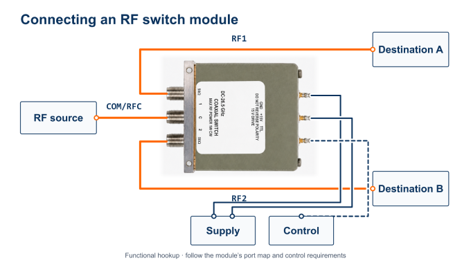
Check the module’s instructions. Confirm the operating band, impedance, RF power limits, supply voltage, and control requirements. Read the port map and truth table to see which connection each command establishes.
Connect the RF paths. With RF output disabled, connect the source to the common port, often marked COM or RFC. Connect the destinations to the branches, often RF1 and RF2. Use compatible cables and follow the instructions for unused ports.
Provide power and control. Connect the specified supply and control interface, following the grounding and power-up sequence. Keep RF output disabled until the module is ready. Use a suitable driver if your controller cannot meet the module’s voltage or current requirements.
Select the required path. For this cold-switching example, disable RF output before each change, apply the required control command, and wait for the documented switching and settling requirements to be satisfied before restoring RF.
Verify operation. Check that the selected branch passes the signal and that leakage at the other branch meets the requirement. Repeat these checks across the required band and in both states. A calibrated vector network analyzer (VNA) can measure transmission and isolation; verify switching and settling times separately if timing matters.
RF Switch Circuit Diagram and Port Configurations
An RF switch circuit diagram shows the RF paths, switching elements, and control or bias connections. The port configuration identifies the connections those paths can establish.
The pole count describes how many circuits are switched. The throw count describes how many connections are available to each circuit.
Configuration | Full name | RF ports | Function |
SPST | Single-pole, single-throw | Two | Connects or interrupts one RF path |
SPDT | Single-pole, double-throw | Three: one common port and two branches | Connects the common port to either branch |
SPnT | Single-pole, multiple-throw | One common port plus n branch ports | Connects the common port to one of n branches |
For example, an SP4T switch has four selectable branches and five RF ports.
An RF A/B switch selects between two feeds or paths, commonly using an SPDT arrangement. A/B describes the selection function; it does not identify the switching technology.
The following schematic illustrates an SPDT PIN-diode switch with a series diode and a shunt diode in each branch.
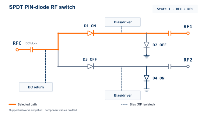
The series diode controls the connection along its branch. The shunt diode connects that branch toward RF ground to help suppress unwanted transmission when the branch is inactive.
In the table, ON means the diode conducts; OFF means it does not conduct.
Conceptual state | Selected connection | RF1 branch | RF2 branch |
State 1 | RFC to RF1 | Series ON; shunt OFF | Series OFF; shunt ON |
State 2 | RFC to RF2 | Series OFF; shunt ON | Series ON; shunt OFF |
Notice that the shunt diode conducts when its branch is inactive. A diode’s conduction state therefore differs from the transmission state of the complete path. States 1 and 2 identify RF connections; the required control voltages depend on the circuit and driver.
How Do RF Switches Support Transmit/Receive and Antenna Switching?
Transmit/receive (T/R) switching and antenna switching are two of the most common RF switch applications.
Both rely on selecting the required signal path while reducing unwanted interaction with inactive circuitry.
Transmit/Receive Switching
A transmit/receive switch allows a transmitter and receiver to share a common antenna.
A typical SPDT arrangement includes:
A common RF port connected to the antenna
A transmit port connected to the power amplifier (PA)
A receive port connected to the low-noise amplifier (LNA)
During transmission, the switch connects the PA to the antenna while isolating the LNA from the high-power transmit signal.
During reception, the switch connects the antenna to the LNA while isolating the transmitter path.
This creates several important engineering requirements.
First, insertion loss in the transmit path must be controlled to preserve available output power.
Second, receive-path insertion loss must be minimized because attenuation ahead of the LNA directly affects receiver sensitivity.
Third, transmit-to-receive isolation must be sufficient to prevent excessive RF energy from reaching sensitive receiver circuitry.
A switch's nominal isolation rating alone does not guarantee adequate receiver protection. The system must also account for reflected signals, transient conditions, and any additional protection or limiting circuits.
Control sequencing is equally important.
The PA may need to be disabled before changing the switch state, and transmission should resume only after the required RF path is established and sufficiently settled.
Antenna Switching
Antenna switching allows one RF transceiver to operate with multiple antennas.
For example, an SP4T switch can connect a common RF chain to one of four antenna branches.
The system may select an antenna according to signal strength, operating band, polarization, or another control condition.
Important requirements include:
Low insertion loss in the selected branch
Sufficient isolation between antenna ports
Appropriate impedance matching
Switching speed compatible with system timing
Consistent phase response where phase-sensitive operation is required
In multi-antenna systems, the physical interconnects must also be considered.
Connectors, PCB transmission lines, and custom RF cable assemblies can introduce additional insertion loss, reflections, and phase differences that influence the installed switching network.
These effects become increasingly important as operating frequency rises.
FAQ
Discussion (0)
Be the first to comment.