How to Measure the Output Impedance of an RF Amplifier?

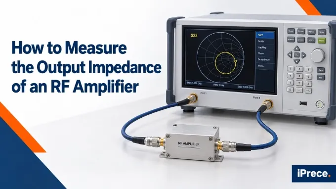
To measure an RF amplifier’s output impedance, use a vector network analyzer to measure its complex S22 parameter. Power the amplifier at its specified bias point and terminate its input with the VNA’s reference impedance, typically 50 Ω. The VNA can display the result as resistance and reactance or on a Smith chart.
Although the basic measurement sounds straightforward, the RF amplifier test setup determines whether the result is accurate—and whether the measurement is safe for the equipment. Unlike a passive device, a powered amplifier can introduce DC, startup transients, oscillation, or unexpected RF power into the measurement path. So before measuring, account for all equipment. These factors affect both measurement accuracy and equipment safety.
RF Amplifier Output Impedance Measurement Setup
A standard VNA amplifier output impedance measurement requires the following equipment:
Two-port VNA: Measures the RF amplifier S22 parameter over the required frequency range. A two-port instrument also ensures that the amplifier input is connected to a defined reference termination during the measurement.
VNA calibration kit: Used to move the measurement reference planes to the ends of the test cables or the amplifier interfaces.
Phase-stable RF test cables: Connect the amplifier without introducing excessive loss or phase variation when the cables move. Custom RF cable assemblies can also reduce unnecessary adapters and transitions.
Adapters and test fixtures: Required when the amplifier connectors or PCB interfaces do not mate directly with the test cables. Their effects must be included in the calibration or removed through de-embedding.
Regulated bias supply: Powers the amplifier at the specified voltage and quiescent current. Current limiting is advisable during initial connection.
Bias tees: Required when DC bias and the RF signal must enter the amplifier through the same port.
DC blocks: Protect the VNA if DC may be present at an amplifier RF port and is not already blocked internally.
Protection components: Receiver attenuation, suitable attenuators, or directional-coupler arrangements may be required if the amplifier can expose the VNA to unsafe RF power.
Basic VNA Connection
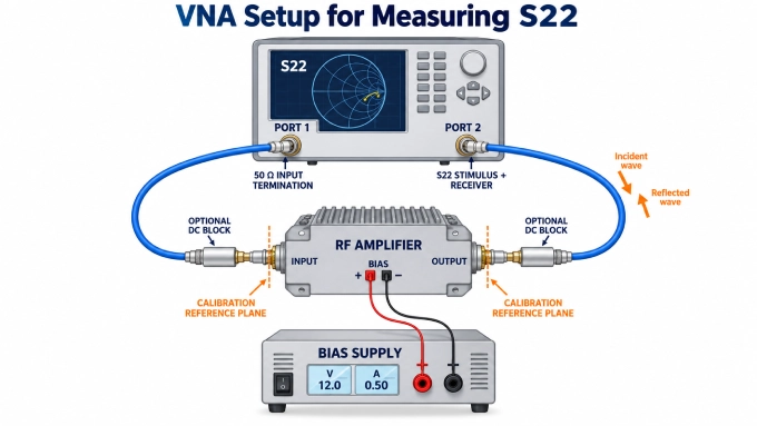
For a conventional two-port measurement, connect the system as follows:
VNA Port 1 to the amplifier input.
Amplifier output to VNA Port 2.
Regulated DC supply to the amplifier’s bias terminals or through the required bias tee.
Heat sink or other specified thermal management attached before applying power.
Keep the following points in mind when arranging the VNA connection:
Understand the port roles: During an S22 measurement, VNA Port 2 sends a low-level test signal toward the amplifier output and measures the reflected wave.
Keep the input properly terminated: Port 1 should present the amplifier input with the VNA’s reference impedance, typically 50 Ω.
Do not drive the input during a standard S22 measurement: Applying a separate RF input signal creates a driven measurement known as hot S22, which requires a different setup.
Define the measurement plane before calibration: For a connectorized amplifier, this is normally at its input and output connectors.
Account for fixtures and PCB structures: With a PCB-mounted or unmatched amplifier, connectors, launches, transmission lines, package parasitics, and bias components may lie between the VNA and the device output. Unless these elements are de-embedded, the VNA measures the impedance of the complete path rather than the amplifier alone.
Measuring the Output Impedance of an RF Amplifier, Step-by-Step
Once the test setup is complete and its power and DC limits have been checked, use the following procedure to measure the amplifier’s complex S22 parameter.
Step 1: Define the Measurement Conditions
Set the conditions under which the amplifier’s output impedance will be characterized. At minimum, record:
Start and stop frequencies.
Number of sweep points.
VNA stimulus power.
IF bandwidth.
Amplifier bias voltage and quiescent current.
Intended operating temperature.
Output impedance can change with frequency, bias, and temperature, so these conditions must remain consistent if the measurement will be compared with simulation data, datasheet values, or later tests.
Step 2: Confirm the Measurement Reference Planes
Use the reference planes selected while planning the test setup. For a connectorized amplifier, these will normally be at the amplifier’s input and output connectors. For a PCB-mounted device, the required plane may be at a fixture interface, package lead, or transistor output.
Any cable, adapter, connector launch, PCB trace, or bias component beyond the calibration plane becomes part of the measured network unless its effect is removed through de-embedding.
Step 3: Set a Safe VNA Power Level
Set the Port 2 stimulus to a level that provides a stable reflection measurement without exceeding the amplifier’s permitted reverse-input power. The signal must also be low enough to maintain small-signal conditions.
Where possible, configure the final measurement power before calibration. Changing the source power significantly after calibration can affect measurement accuracy on some VNAs.
Step 4: Calibrate the VNA
Perform an appropriate two-port calibration over the selected frequency range. For a connectorized measurement, a full two-port SOLT calibration is commonly used to place the reference planes at the ends of the test cables.
If a PCB fixture or non-coaxial interface separates the calibration plane from the amplifier, use an appropriate fixture-removal or de-embedding method. After calibration, avoid bending, twisting, or repositioning the phase-stable test cables.
Step 5: Connect and Bias the Amplifier
Disable the VNA output and confirm that the bias supply is off before connecting the amplifier. Then:
Connect VNA Port 1 to the amplifier input.
Connect the amplifier output to VNA Port 2.
Tighten coaxial connectors to the specified torque.
Connect the bias supply through the amplifier’s DC terminals or bias tee.
Attach the required heat sink or other thermal management.
Apply bias using the sequence specified by the amplifier manufacturer.
Check that the measured supply current is close to the expected quiescent current. Allow the amplifier to reach a stable operating temperature before beginning the sweep.
During the S22 measurement, Port 1 must present the amplifier input with the VNA’s reference impedance. Do not apply a separate RF drive signal to the input during this standard small-signal procedure.
Step 6: Check for Unexpected Output Power
Before starting the measurement, confirm that the amplifier is not oscillating and that no RF or DC level at either port exceeds the VNA’s limits. Unexpected bias current, unstable readings, or measurable output without an intentional input signal may indicate oscillation.
If the amplifier can produce enough power to damage or compress the VNA receiver, stop the test and use a properly designed high-power measurement arrangement. An ordinary attenuator or coupler should not be added after calibration without accounting for its effect on the measurement.
Step 7: Measure the Complex S22 Parameter
Select S22 on the VNA and begin the frequency sweep. In this measurement, Port 2 applies the incident signal to the amplifier output and measures the reflected signal, while Port 1 provides the required input termination.
Display the result using one or more of the following formats:
S22 magnitude and phase.
Log-magnitude output return loss.
Smith chart.
Resistance and reactance.
Complex impedance.
Calculating output impedance from S22 requires both magnitude and phase; Return loss or VSWR alone are insufficient. This illustrates a key difference between a VNA and a spectrum analyzer: a VNA measures complex reflection, while a conventional spectrum analyzer with a tracking generator and reflection bridge measures reflection magnitude only.
Step 8: Save and Verify the Measurement
Save the complex S22 data together with the test conditions, including bias, temperature, stimulus power, frequency range, calibration method, reference planes, and fixture configuration.
Repeat the sweep and check that the trace remains stable. Movement between repeated sweeps can indicate thermal drift, cable movement, connector instability, oscillation, or changes in the amplifier’s bias point. Once the measurement is repeatable, the complex S22 data can be converted into the amplifier’s small-signal output impedance.
How to Convert S22 to Output Impedance
S22 is a complex reflection coefficient rather than an impedance value. Once its magnitude and phase have been measured, convert it to output impedance using:
Here, is the VNA’s reference impedance, normally 50 Ω. The calculation must use the complex form of S22, including both magnitude and phase. Most VNAs can perform this conversion automatically and display the result on a Smith chart or directly as resistance and reactance.
For example, suppose a 50 Ω VNA measures:
Substituting this value into the equation gives:
The result indicates approximately 46.2 Ω of resistance and 19.2 Ω of capacitive reactance at that frequency. Because S22 varies across the sweep, output impedance should normally be reported as versus frequency rather than as one fixed value.
S22 can also be expressed as output return loss:
For , the output return loss is approximately:
Return loss describes the magnitude of the output mismatch, but it cannot identify the complex output impedance because it contains no phase information. For example, produces the same 14 dB return loss but corresponds to approximately —an inductive rather than capacitive impedance.
Common RF Amplifier Output-Impedance Measurement Errors
Common errors include:
Measuring the amplifier without its specified bias voltage and quiescent current.
Applying enough VNA stimulus power to drive the amplifier outside its small-signal region.
Allowing amplifier output power or DC voltage to reach an unprotected VNA port.
Failing to check the amplifier for oscillation or unexpected output power.
Calibrating at a reference plane different from the required impedance plane.
Ignoring adapters, fixtures, connectors, PCB traces, or test cables beyond the calibration plane.
Moving phase-sensitive test cables after calibration.
Converting only the magnitude of S22 and ignoring its phase.
Treating output impedance as a constant rather than a frequency-dependent quantity.
Confusing S22-derived output impedance with a recommended or optimum load impedance.
Assuming that small-signal S22 represents amplifier behavior near compression or saturation.
Can S22 Be Used for RF Amplifier Output Matching?
Yes—but primarily for small-signal matching under defined operating conditions. S22 describes the reflection seen looking into the amplifier’s output while its input is terminated in the VNA reference impedance. After converting S22 to output impedance, that impedance can serve as the starting point for an output matching network.
When S22 Is Sufficient
S22 can guide output matching when:
The amplifier operates in its linear, small-signal region.
The bias, frequency, temperature, and input termination match the intended operating conditions.
Reverse transmission from output to input is sufficiently small.
The amplifier remains stable with the proposed source and load impedances.
Under these conditions, the matching network can transform the external 50 Ω load so that the amplifier sees the conjugate of its measured output impedance.
When S22 Alone Is Not Sufficient
S22 should not be treated as an independent, fixed output impedance when reverse transmission, represented by S12, is significant. Changing the source impedance at the amplifier input can then change the reflection seen at its output.
Simultaneous input and output matching may therefore require:
All four S-parameters: S11, S21, S12, and S22.
Stability analysis over the relevant frequency range.
Evaluation of the proposed source and load reflection coefficients.
S22 is also insufficient for finding the optimum load of a power amplifier operating near compression or saturation. Under large-signal conditions, the best load depends on the design objective, such as output power, efficiency, gain, or linearity. Load-pull testing is normally used to identify that impedance.
Measured Output Impedance vs. Recommended Load Impedance
These two values should not be treated as interchangeable
S22-derived output impedance: The small-signal impedance looking into the amplifier output under specified bias and input-termination conditions.
Recommended or optimum load impedance: The load that should be presented to the device to achieve a target such as maximum power, efficiency, or linearity. It may come from load-pull testing, simulation, or the manufacturer’s datasheet.
For a nonlinear power amplifier, the recommended load impedance is not necessarily the conjugate of the output impedance calculated from small-signal S22.
Account for the Complete Output Network
For an unmatched amplifier, the output matching network transforms the external 50 Ω load into the required impedance at the device plane. The final design must include the RF behavior of:
Package parasitics.
PCB transmission lines and connector launches.
Inductors and capacitors, including their parasitics and self-resonance.
Bias inductors, RF chokes, bypass capacitors, and other bias-network elements.
S22 is therefore a useful starting point for linear small-signal matching, but it is not a universal substitute for four-port S-parameter analysis, stability analysis, or large-signal load-pull measurements.
Measuring the Output of a Driven Power Amplifier
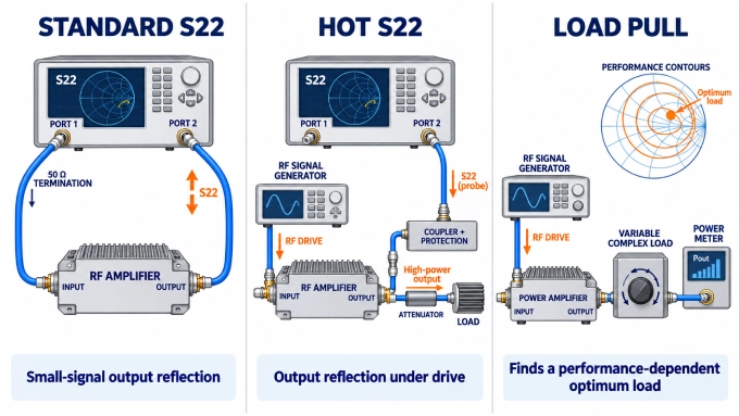
Standard S22 measurement characterizes the amplifier under small-signal conditions without a separate drive signal applied to its input. When the goal is to characterize a power amplifier under normal driven operation, hot S22 or load-pull measurements may be required.
Hot S22
Hot S22 measures the output reflection coefficient while the amplifier is actively driven. Because the amplifier’s own output signal can be much stronger than the VNA’s reverse test signal, the setup may require couplers, attenuation, receiver protection, and frequency-offset techniques to separate the signals and prevent receiver compression or damage.
Hot S22 characterizes output reflection under drive, but it does not automatically identify the load that produces the best amplifier performance.
Load-Pull Measurement
Load-pull testing presents a range of complex load impedances to the amplifier and records the resulting output power, gain, efficiency, or linearity. The results are commonly plotted as performance contours on a Smith chart.
Unlike standard S22 measurement, load pull finds an optimum load for a particular performance objective. The optimum impedance for maximum output power may differ from the impedance that provides the best efficiency or linearity.
FAQ
Discussion (0)
Be the first to comment.